Handbook of Modern Coating Technologies
Functional layers used in integrated microelectronic circuits
Interface effects in integrated circuits (ICs) are becoming increasingly important while downsizing of microelectronics. The fabrication of these devices frequently involves multilayer structures stacking different materials (metals, dielectrics) on a silicon substrate followed by mechanical—chemical polishing. Delamination at a particular interface during this process is obviously a serious problem in manufacture. As an example of the usefulness of NR we will review a recent study on the interface between amorphous carbon (a-C) and SiO2, which is
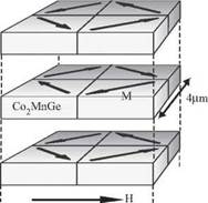
| FIGURE 4-13 Example of a domain structure as extracted from the specular and off-specular polarized neutron reflectivity data. The domains show antiferromagnetic coupling between the layers with the magnetization pointing along four discrete directions in each individual layer. Adapted from A. Bergmann, J. Grabis, B.P. Toperverg, V. Leiner, M. Wolff, H. Zabel, et al., Antiferromagnetic dipolar ordering in [Co2MnGe/V] N multilayers, Phys. Rev. B 72 (2005) 214-403. |
often present in ICs and turned out to be the weakest interface during the polishing procedure [49]. Two samples where studied by a combination of NR and XRR both consisting of a 20-nm thick SiO2 layer on top of a 100-nm a-C layer deposited on a silicon wafer. The difference between the two samples studied was the process used to grow the SiO2 layer. For the first sample (S1) the precursors used were SiH4 + CO2 + H2, while for the other sample (S2) only SiH4 + CO2 was used. These two samples showed qualitative differences in the adhesion of the deposited layers. Sample 1 showed severe delamination, whereas sample 2 did not delaminate. As NR is particularly sensitive to the presence of hydrogen which is practically invisible for X-rays a combination of both techniques was be used to measure the mass density and hydrogen concentration in these samples independently. This is illustrated in Fig. 4-14 where the SLD of the NR measurement is shown for the two samples (black squares in A and B) together with the result from XRR measurements on the same samples converted to neutron SLD's assuming no hydrogen (red circles in A and B). A SLD depleted layer between the a-C and SiO2 is observed for the neutron data of sample 1 (Fig. 4—14A), which is not detected by XRR. This is interpreted as an accumulation of hydrogen resulting in the weaker interface of this sample when compared with the second sample, where this interfacial layer is less pronounced (Fig. 4—14B). From the difference of the NR and XRR measurements the hydrogen concentration can be deduced, which is plotted in Fig. 4— 14C.
Another combined study of NR and XRR on the a-C layer revealed the hydrogen distribution in a-C as a function of the annealing process. The authors conclude that H plays a significant role in pacification of the amorphous Si layer [50] important for photovoltaic applications.
The preparation of insulating layers in ICs often implies plasma etching leading to porous materials (e.g., low-k material). NR proved to be very powerful in determining solvent penetration into these porous materials due to the contrast enhancement by using deuterated solvents [51].
| Distance from interface (A) |
| Distance from interface (A) |
| Distance from interface (A) |

FIGURE 4-14 SLD profiles of the two SiO2/a-C interfaces as determined by NR (blacksquares) and the equivalent neutron SLD profiles deduced from XRR (red circles) and their difference (blue triangles). (A) Sample 1 produced using hydrogen in the precursor, (B) sample 2 with no hydrogen gas in the precursor, and (C) hydrogen concentration for the two samples (black squares: sample 1 and red circles: sample 2). a-C, Amorphous carbon; NR, neutron reflectometry; SiO2, silicon oxide; SLD, scattering length density; XRR, X-ray reflectivity. Adapted from J. Segura-Ruiz, P. Gutfreund, G. Imbert, A. Ponard, R. Cubitt, Hydrogen accumulation as the origin of delamination at the a-carbon/SiO2 interface, J. Appl. Phys. 117 (21) (2015) 215302.